2026 IEEE SYMPOSIUM ON VLSI TECHNOLOGY IMAGES AND CAPTIONS
Selected images from the highlighted papers are presented individual high-resolution image files.
Technology Papers
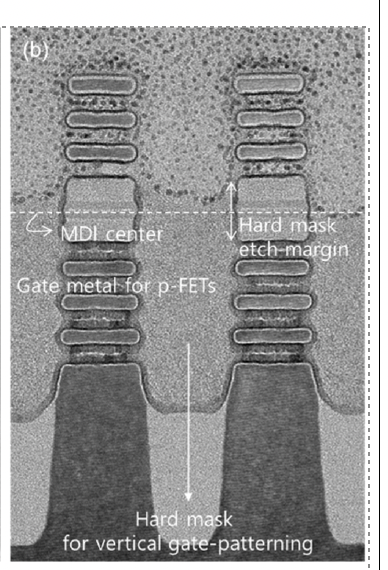
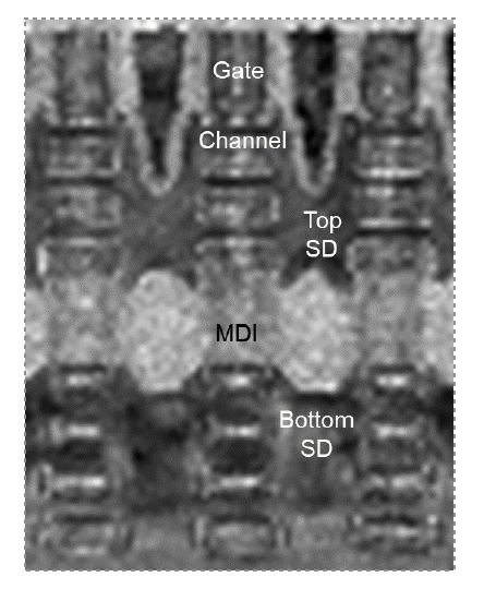
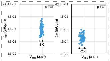
Paper T1.1, “First Demonstration of 3D Stacked FETs at Gate Pitch of 42nm Featuring Triple Stacked Nanosheet Channels for Advanced Logic Applications,” Donghoon Hwang et al, Samsung Electronics
Download documents and images
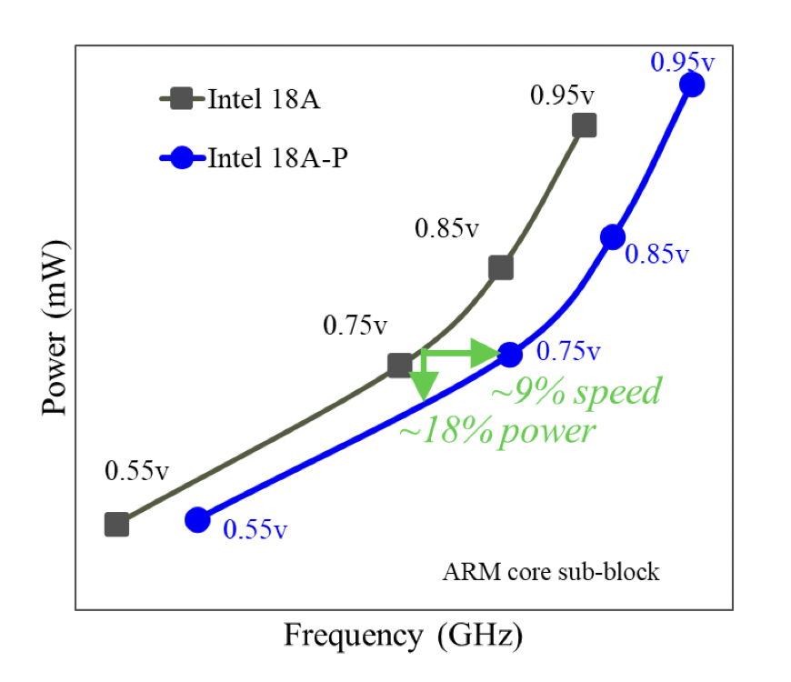
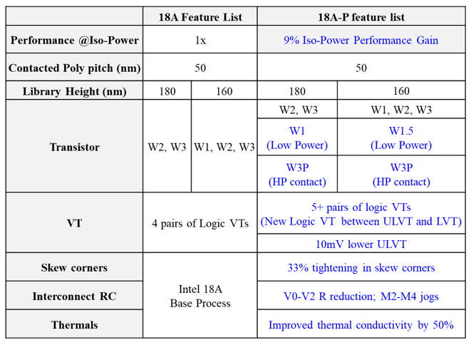
Paper T1.2, “Intel 18A-P CMOS Technology Enhancement Featuring Advanced RibbonFET (GAA) Transistors and PowerVia for High-Performance Computing,” A. Bowonder, et al, Intel Foundry
Download documents and images
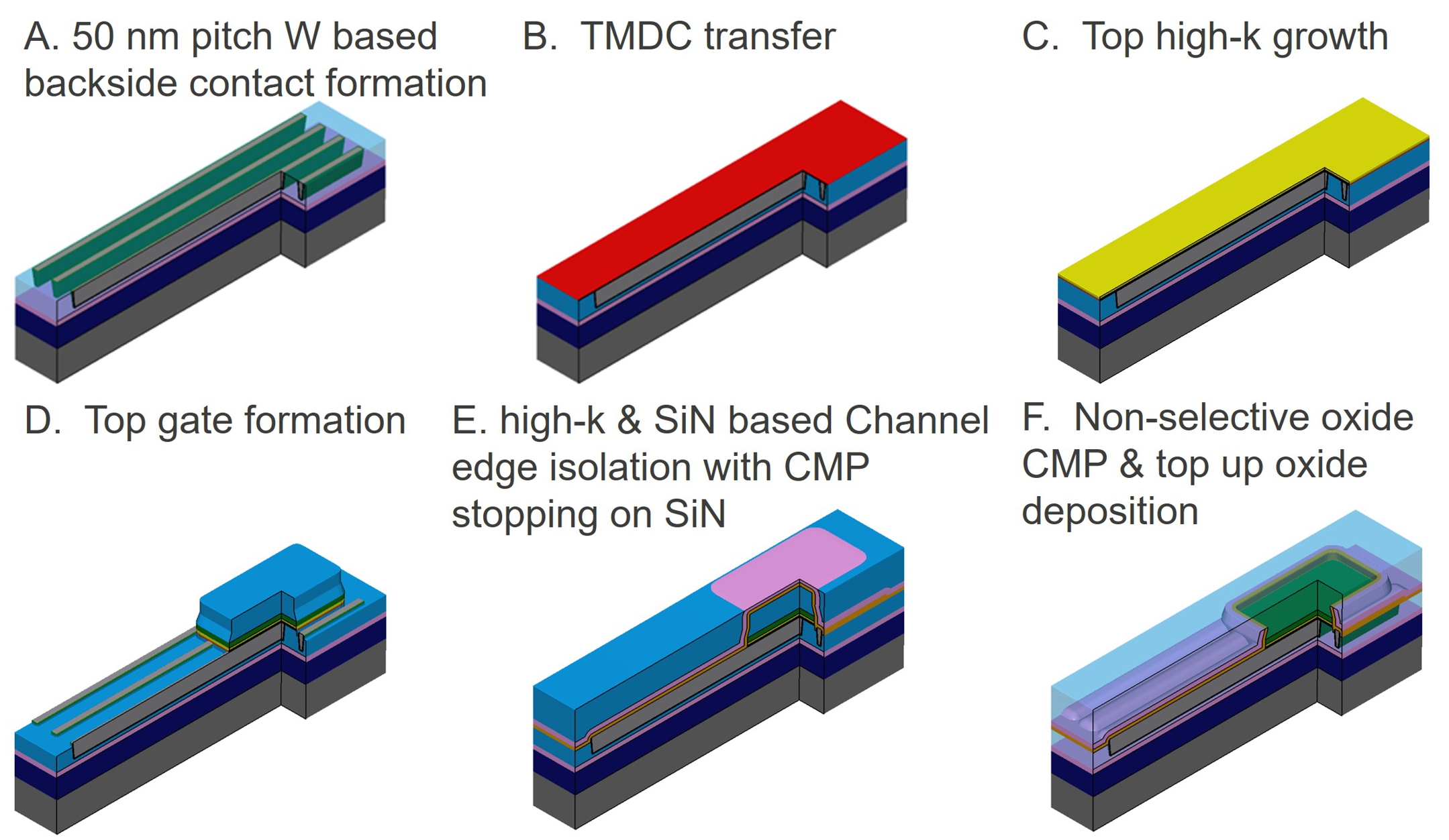
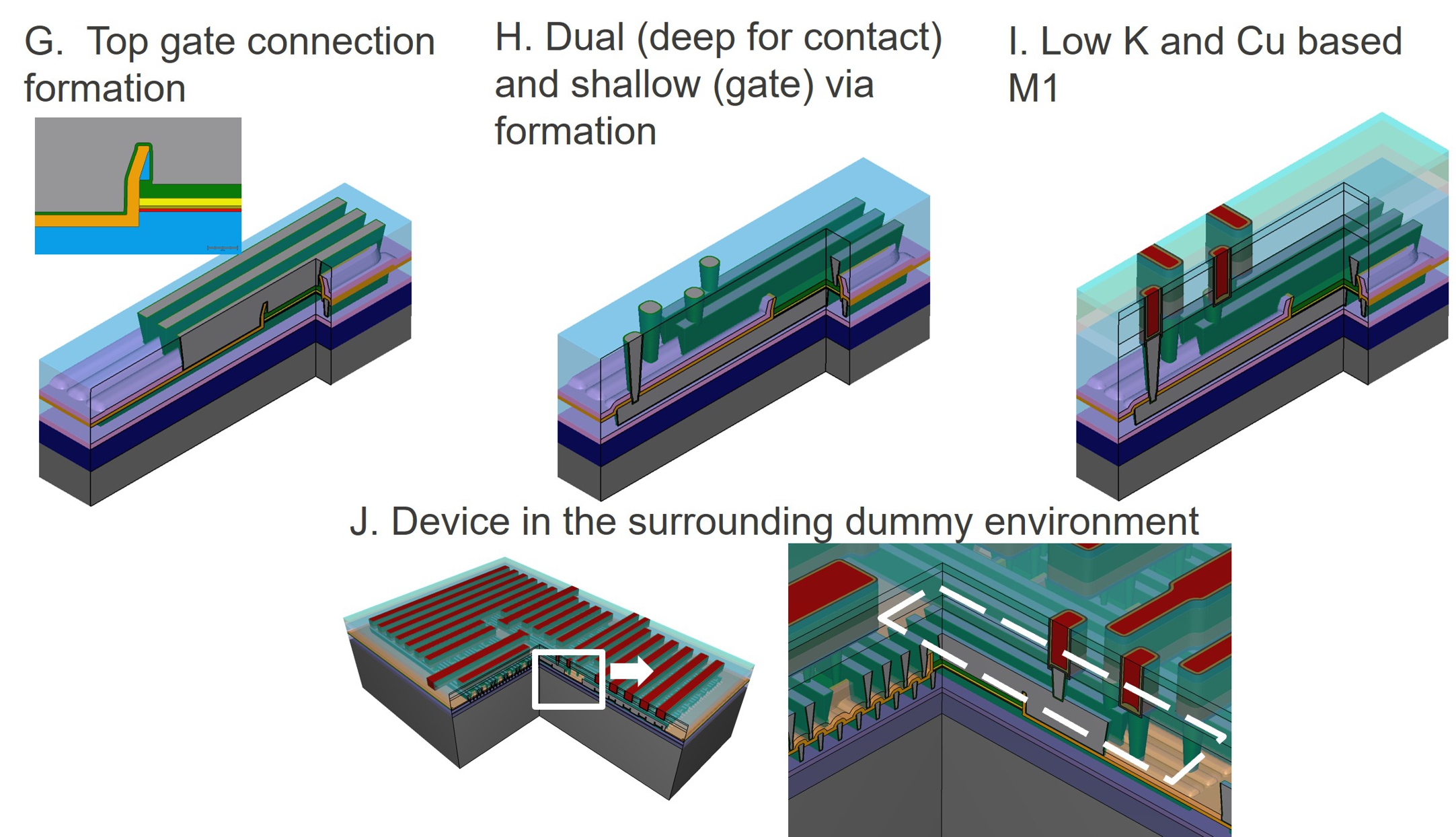
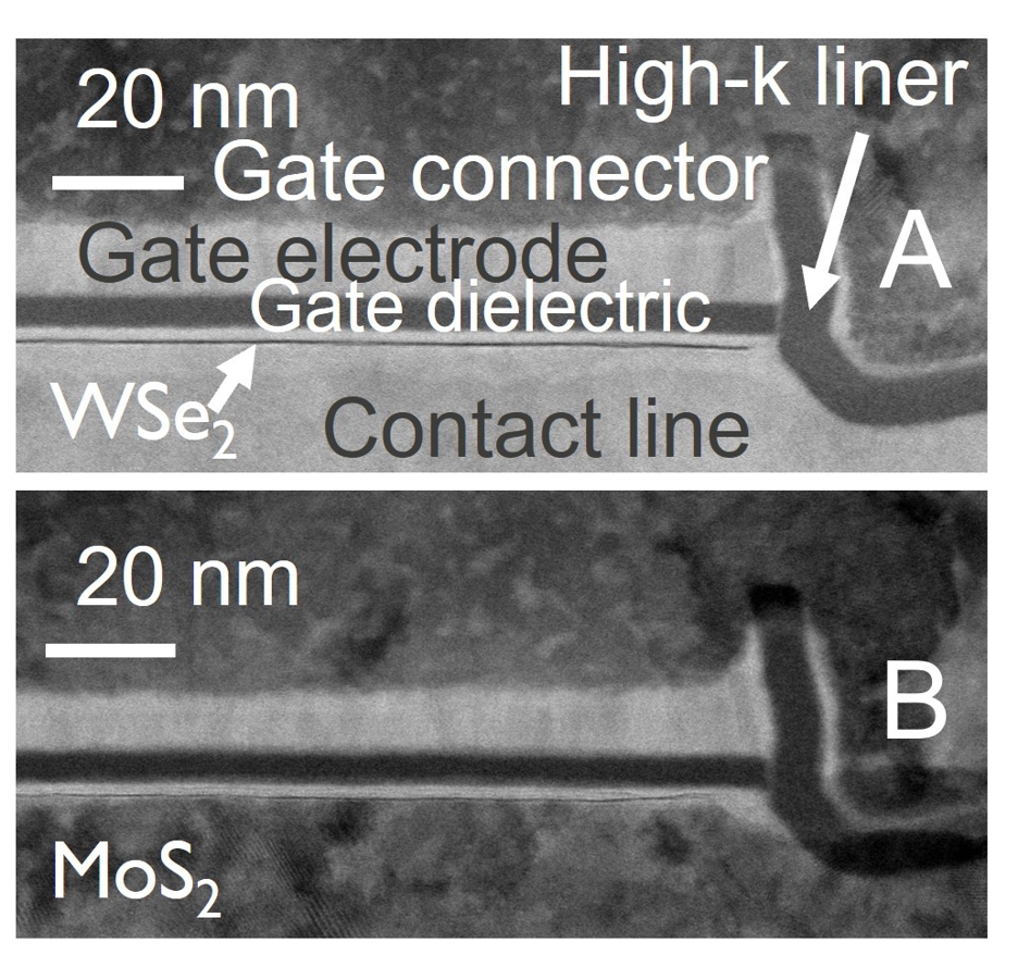
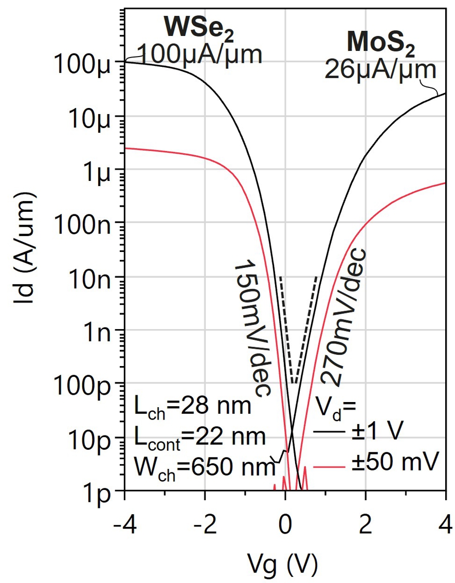
Paper T1.3, “First EUV-enabled Integration Route for 50nm Pitch N and PMOS Transistors with 2D Materials Channel from a 300mm Fab,” T. Schram, imec
Download documents and images
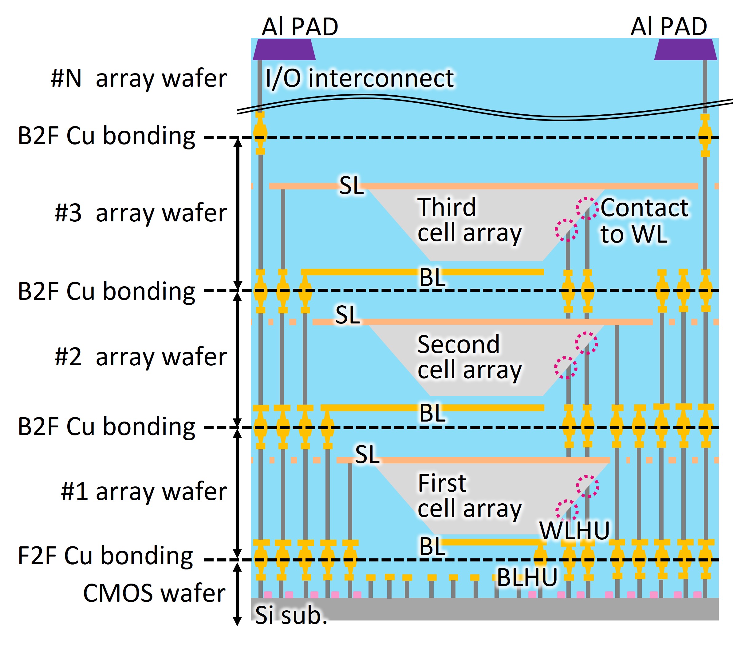
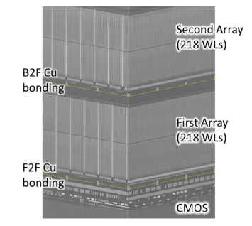
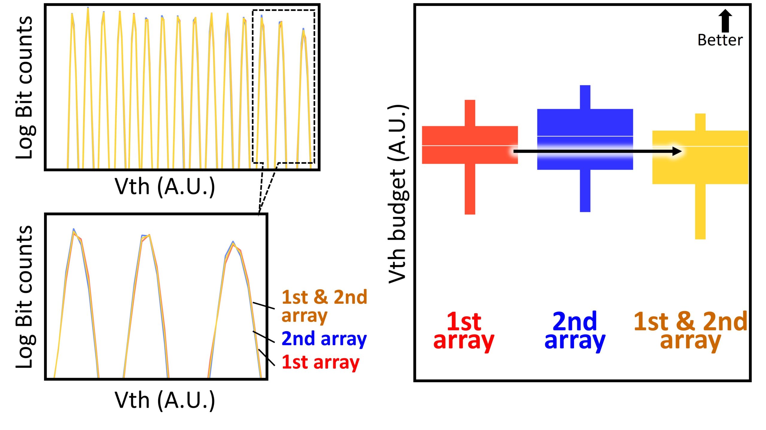
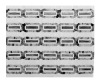
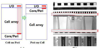
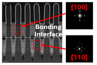
Paper T1.4, “A Multi-Stacked Cell Array Architecture with Wafer-to-Wafer Cu Direct Bonding for Ultra-High-Density 3D Flash Memory beyond 1,000 Word Lines,” M. Noda et al, Kioxia Corporation
Download documents and images
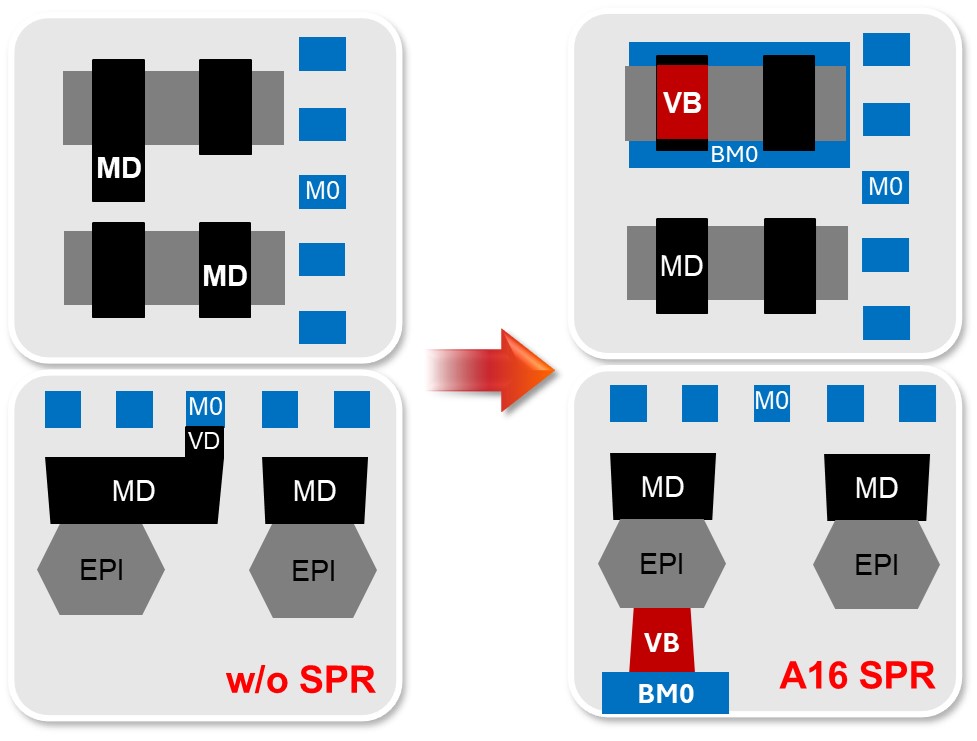
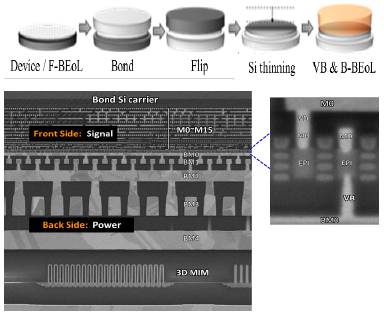
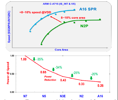
Paper T1.5, “A16 Angstrom-class CMOS Technology featuring Enhanced Nanosheet Transistors with SuperPower Rail (backside direct contact power delivery) for AI and HPC Applications”, G. Yeap et al, TSMC
Download documents and images
Paper T5.1, “Vertically Stacked DRAM Technology for Scaling Evolution,” S.U. Han, Samsung Semiconductor
Download documents and images
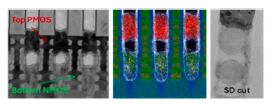
Paper T5.2, “Demonstration of CFET Inverters on Si (110) with 2X2 RibbonFETs at 45nm Gate Pitch with PowerVia and Direct Backside Contacts,” J. A. Wiedemer et al, Intel Corporation
Download documents and images
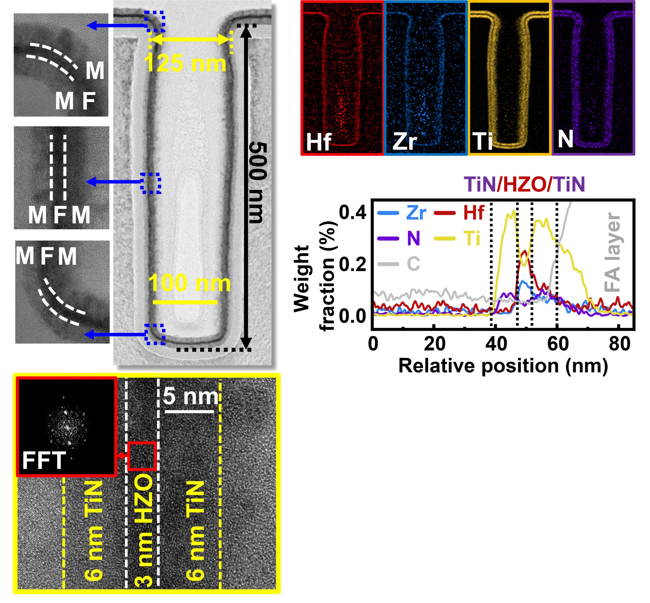
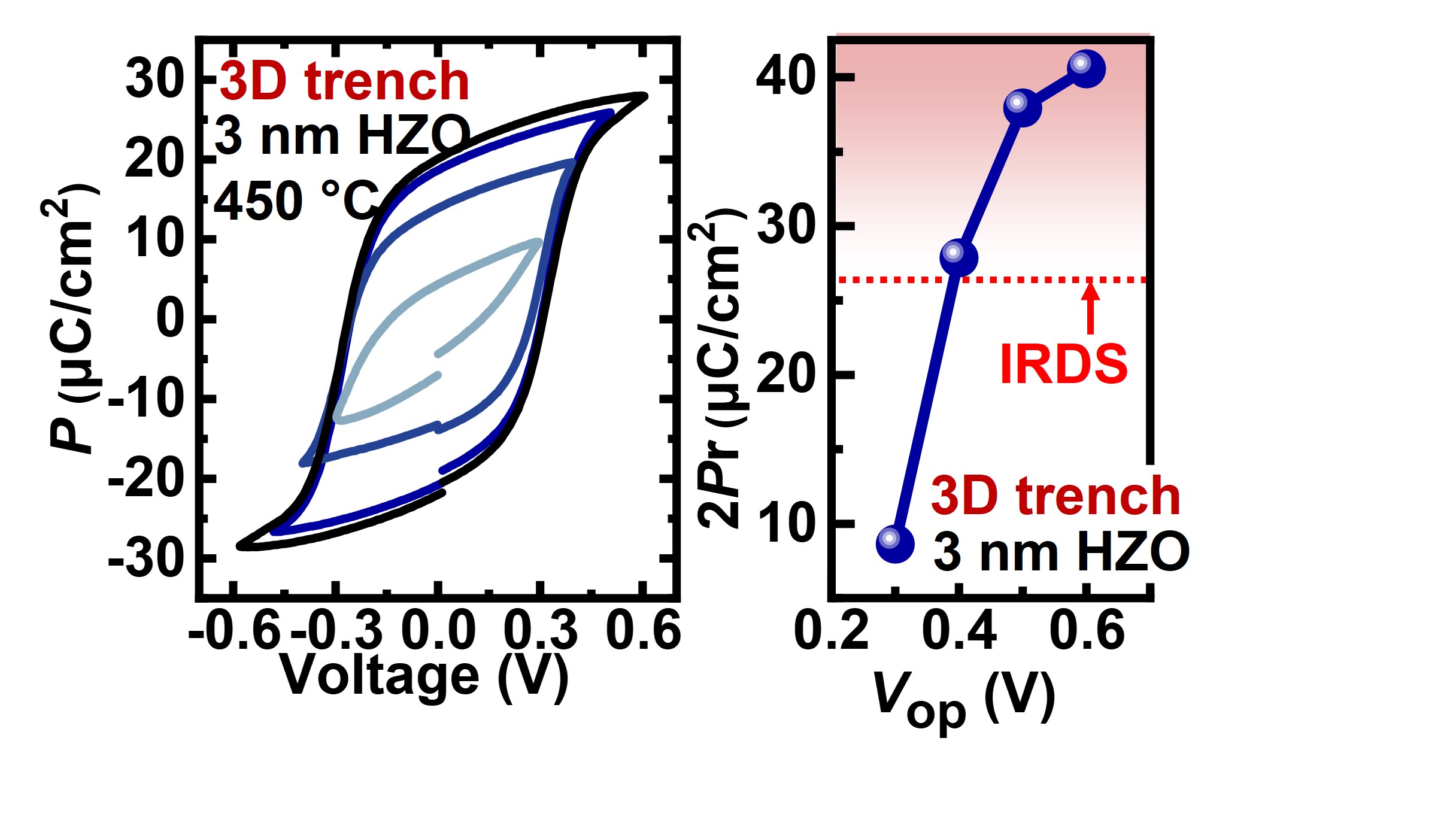
Paper T5.3, “Record 2Pr (>38μC/cm2 at 0.5 V, >28μC/cm2 at 0.4V) of 3D MFM Capacitors Enabled by 3nm HZO and ALD-TiN Orientation Engineering, Y. Feng et al, Shandong University
et al, Intel Corporation
Download documents and images
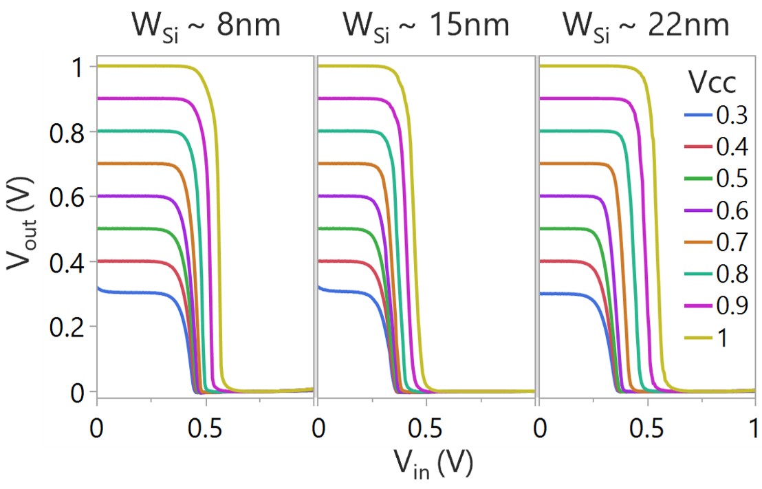
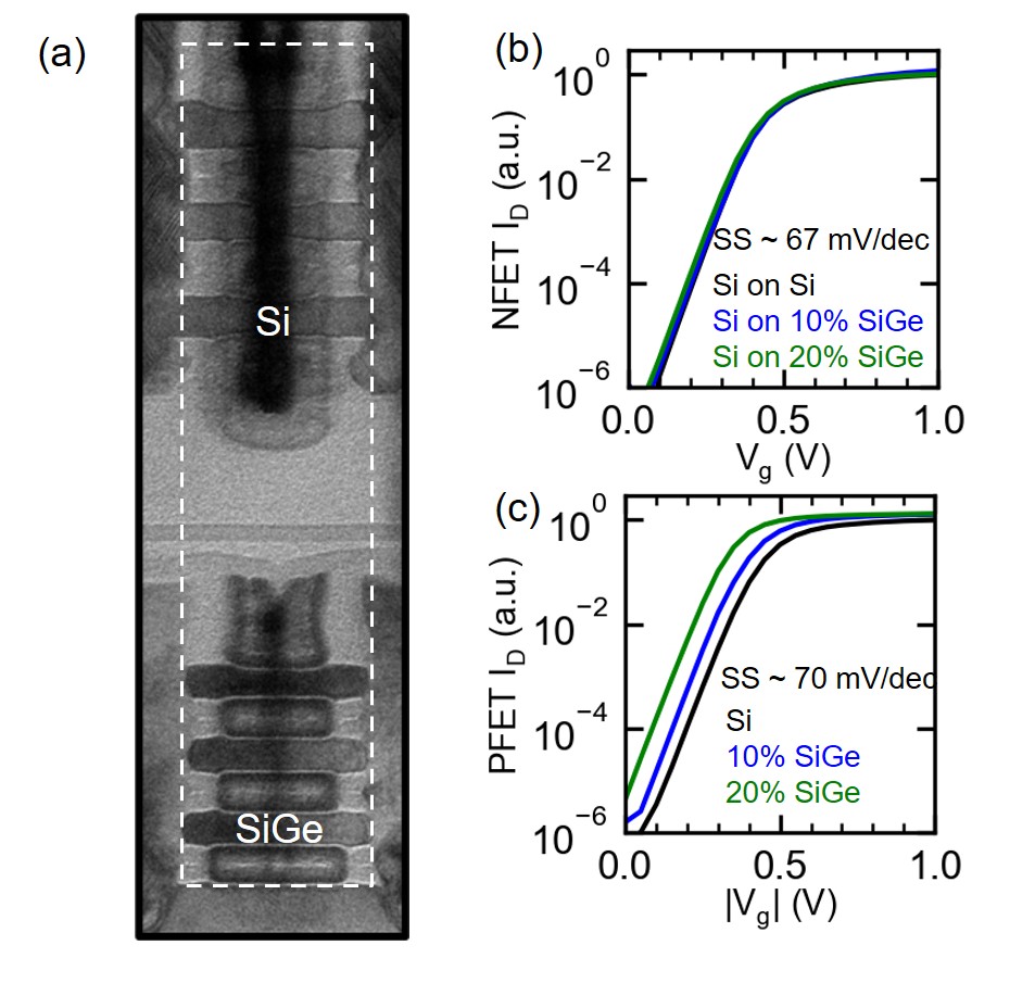
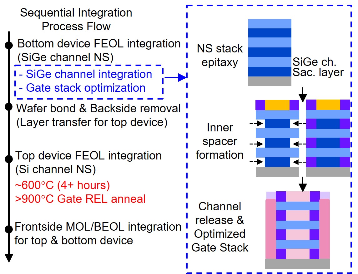
Paper T5.4, “High-Temperature Resilient SiGe Nanosheet PFET RMG Towards Multi-Tiered Sequential Integration,” N. Shanker et al, IBM Research
Download documents and images
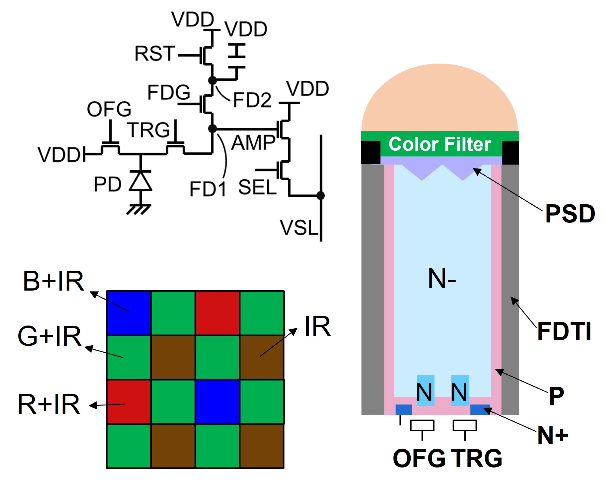
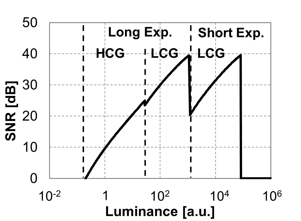
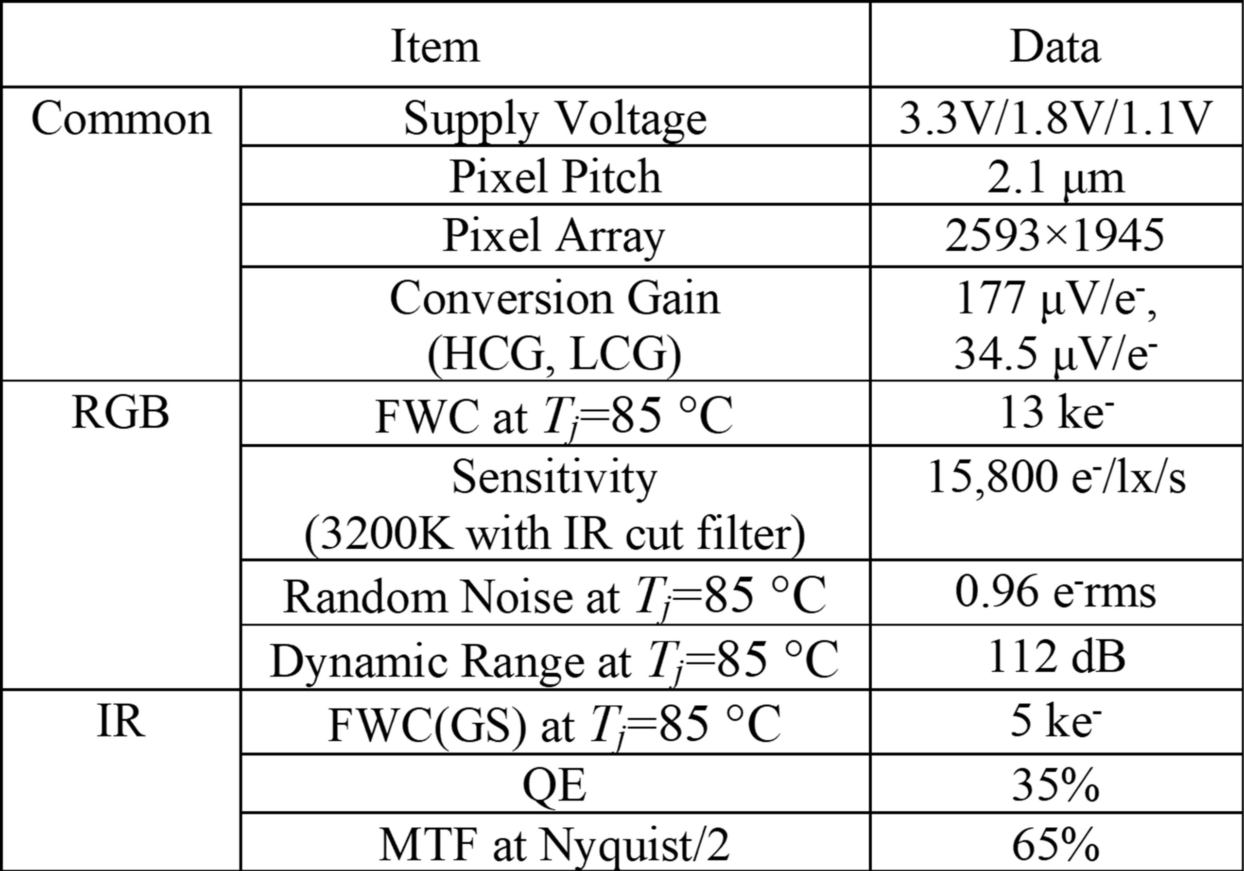
Paper T5.5, “A 2.1-μm Pixel-Pitch CMOS Image Sensor with 65% MTF/35% QE IR Global Shutter and RGB Rolling Shutter Sequential Operation for In-cabin Applications,” M. Hiroki, Sony Semiconductor
Download documents and images
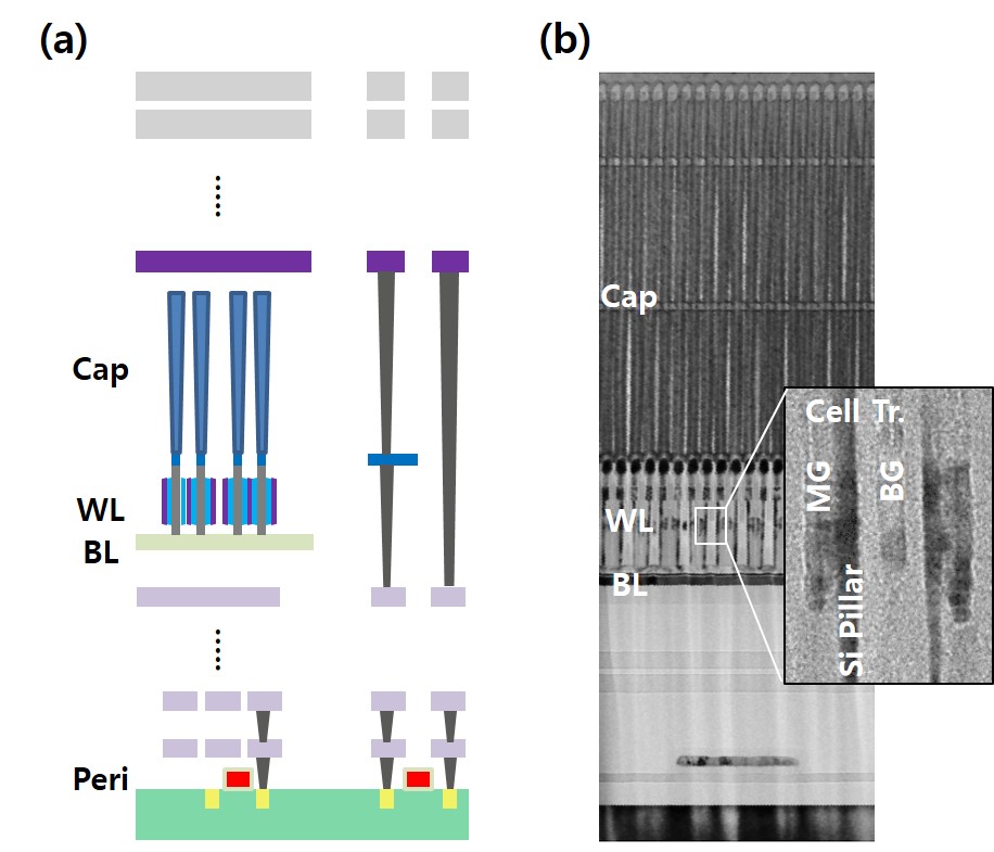
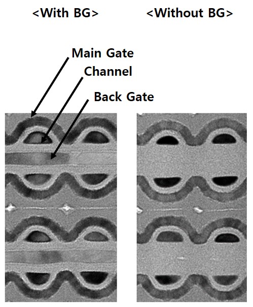
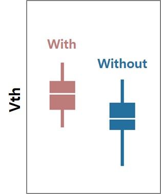
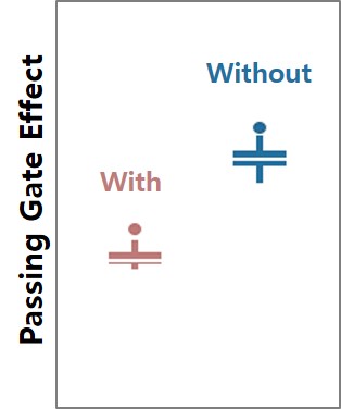
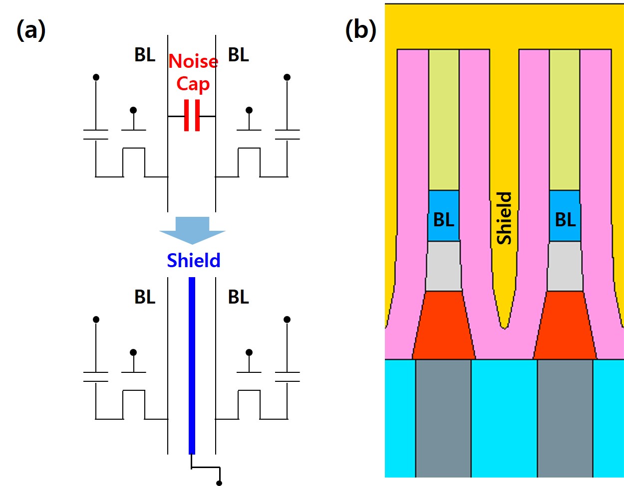
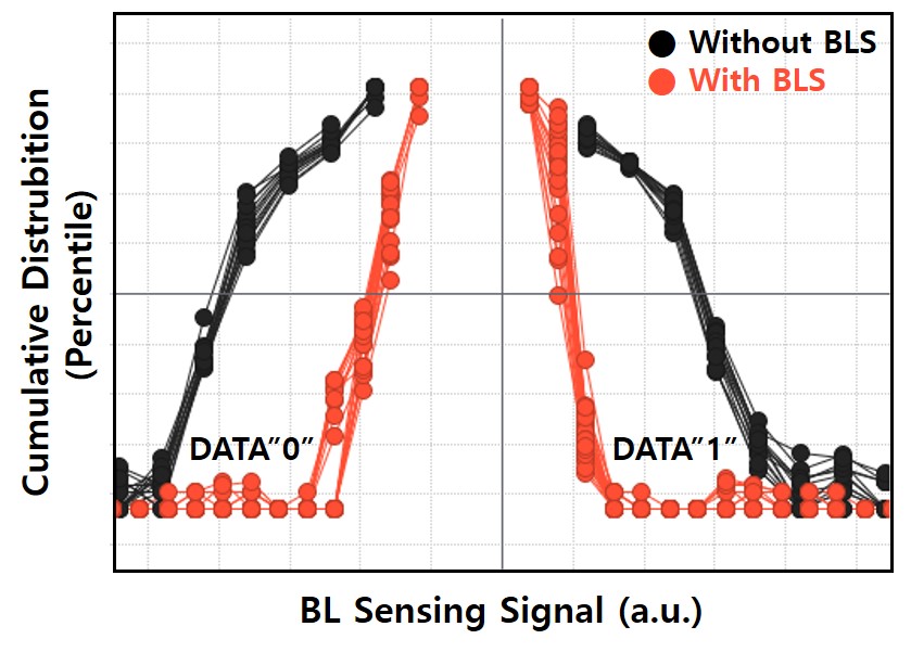
Paper T8.5, “Electrical Characteristics of the 4F2 Vertical Gate (VG) DRAM integrated with BitLine Shielding (BLS) and Back Gate (BG) Transistor,” S. W. Chu et al, SK Hynix
Download documents and images
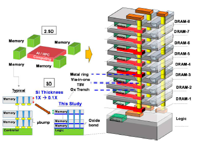
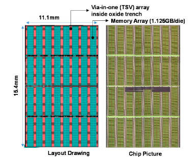
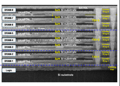
Paper T17.5, “Multiple-Wafer (9-layer), Extreme thin (3µm-Si per stack) and Innovative Fusion-bonded Via-in-one Architecture for High Bandwidth 3D Memory,” C.- L. Lu et al, SAIMEMORY Corporation
Download documents and images
Circuits Papers
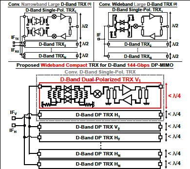
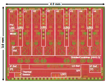
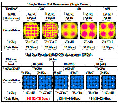
Paper C1.5, “A 144Gbps D-Band Dual-Polarized MIMO High-Density Phased-Array Transceiver in 65nm CMOS for 6G UE,” 22Yudai Yamazaki et al, Institute of Science Tokyo
Download documents and images
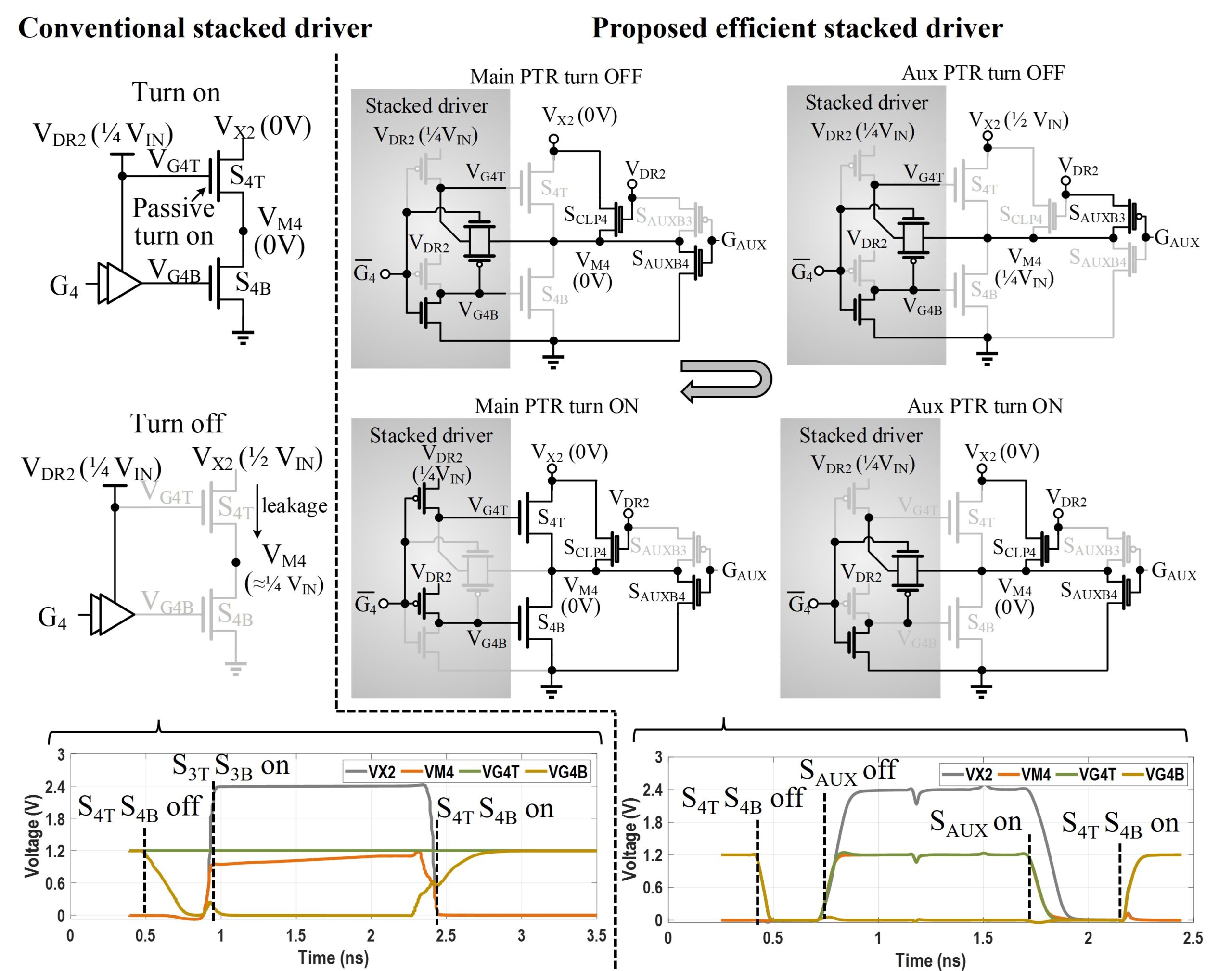
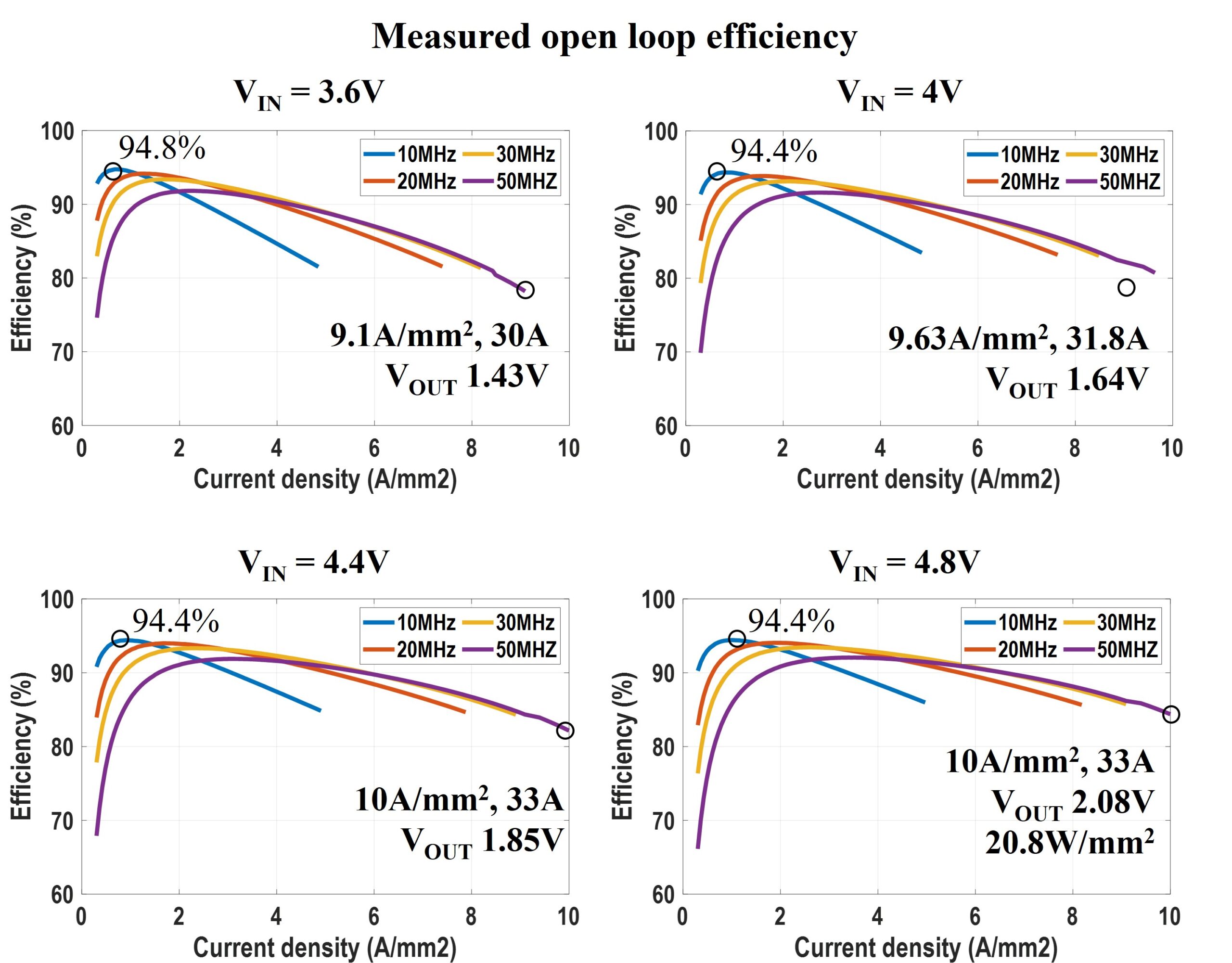
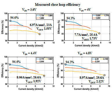
Paper C2.1, “A Monolithic 20W/mm2 4.8V Input 94.8% Peak Efficiency 2-1 Switched Capacitor Voltage Regulator as First-Stage Current Multiplier for Vertical Power Delivery,” M. Gong et al, Intel
Download documents and images
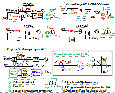
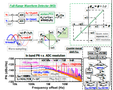
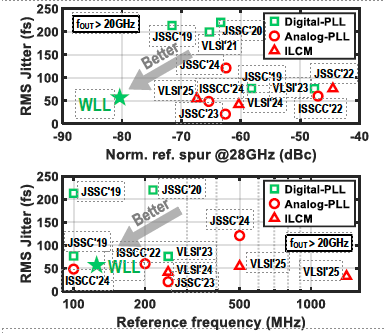
Paper C4.4, “A 28-GHz Quadrature LO-Phase-Shifting Digital Wave-Locked Loop (WLL) Achieving 57.2-fsrms Jitter, −80.6-dBc Spurref, and 0.59µs Near-Integer Lock Time,” Feifan Hong et al, University College Dublin
Download documents and images
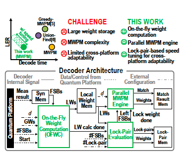
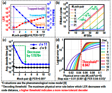
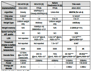
Paper C7.3, “A Full-MWPM Surface Code Decoder with On-the-Fly Weight Computation and Cross-Platform Adaptability Achieving 1.9×10⁻⁶ LER and 20.8-ns Decode Time at 4K,” H. Lyu and Y. Chen et al, Southern University of Science and Technology
Download documents and images
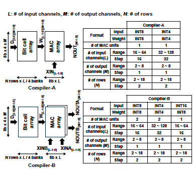
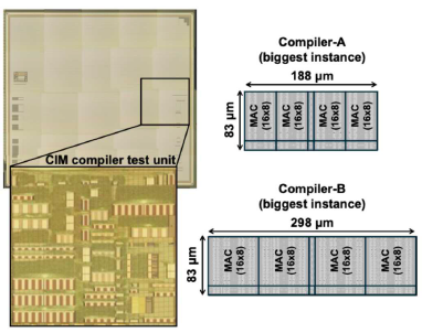
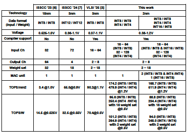
Paper C8.1, “A 2nm 234.4TOPS/W and 511.9TOPS/mm² Digital Computing-in-Memory Compiler with Multiple MAC Units per Weight and Multiple Data Format Support,” Hidehiro Fujiwara et al, TSMC
Download documents and images
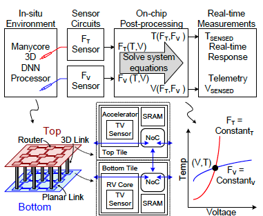
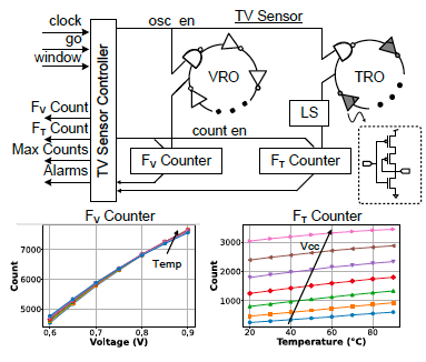
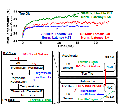
Paper C10.5, “Unified Digital Thermal-Voltage Sensor for Thermal Management in Intel 18A/Intel 3,” Shanshan Xie et al, Intel Corporation
Download documents and images
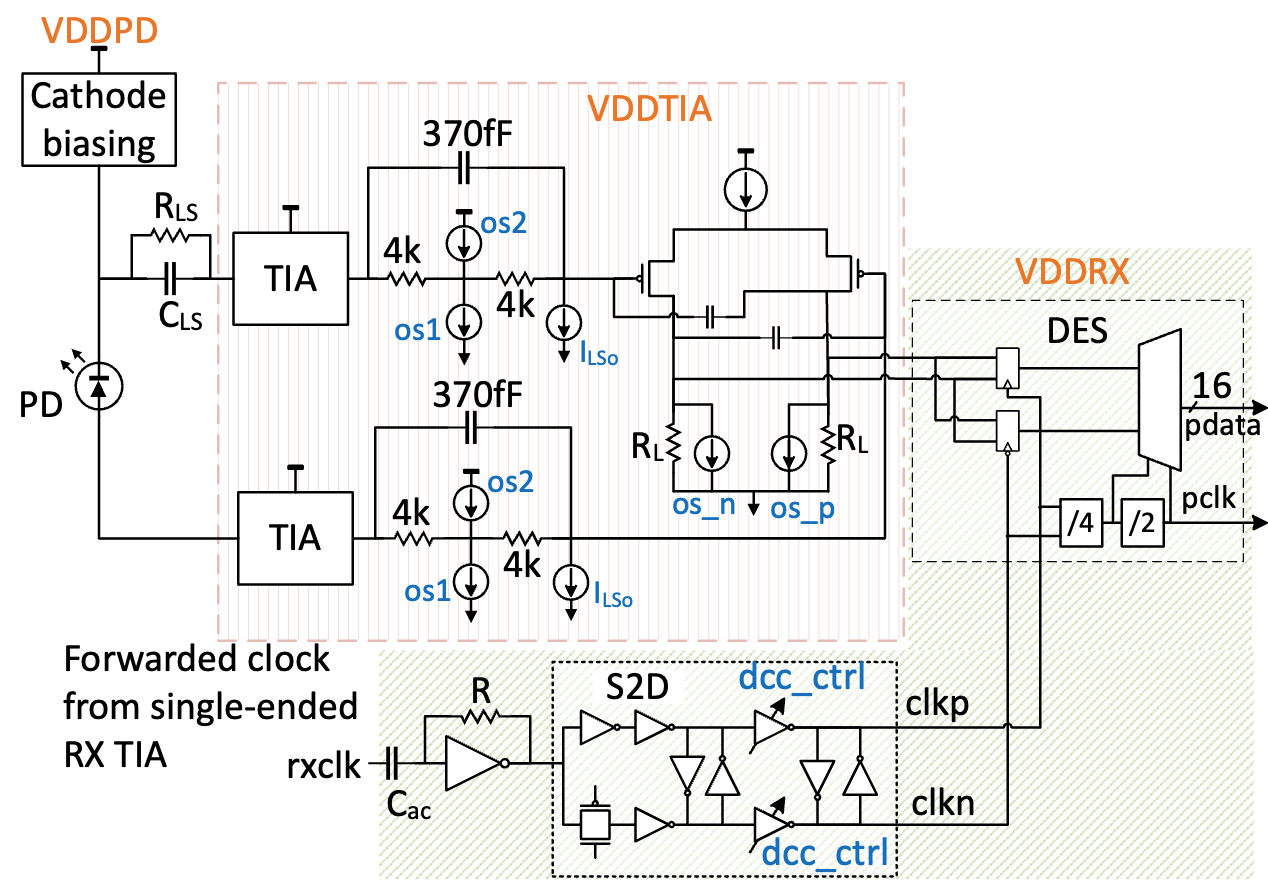
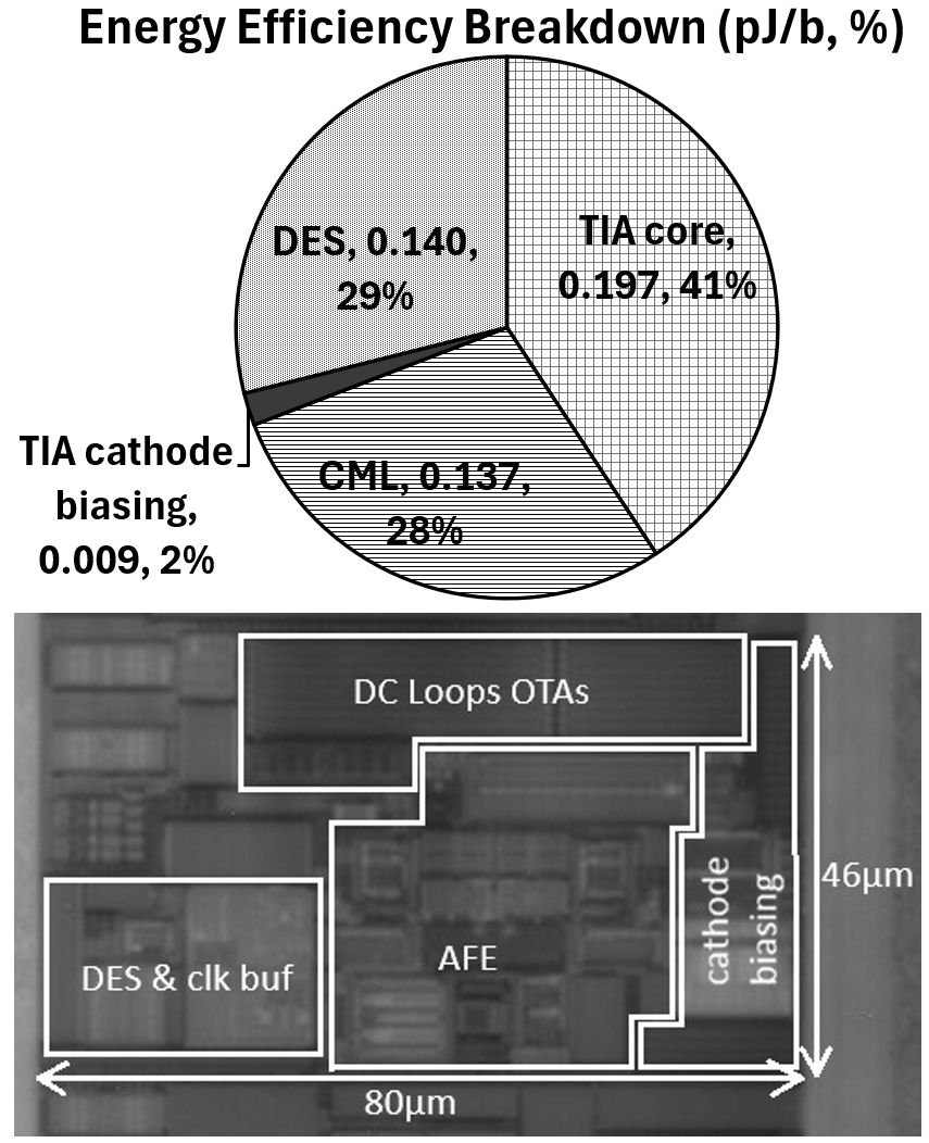
Paper C20.2, “A 32Gb/s Optical Receiver utilizing a Differential TIA with -17.3dBm Sensitivity in a3D-stacked Silicon Photonics Platform,” G. Kalogerakis et al, NVIDIA
Download documents and images
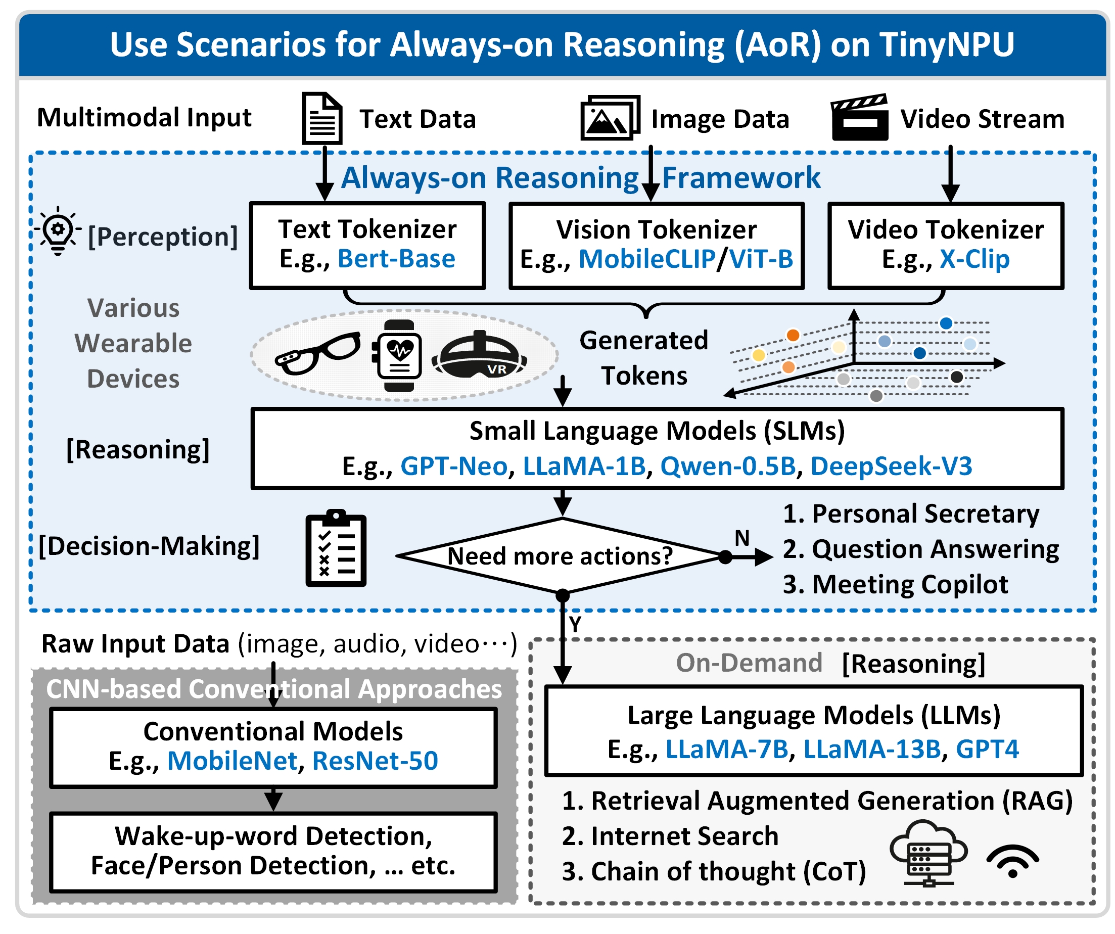
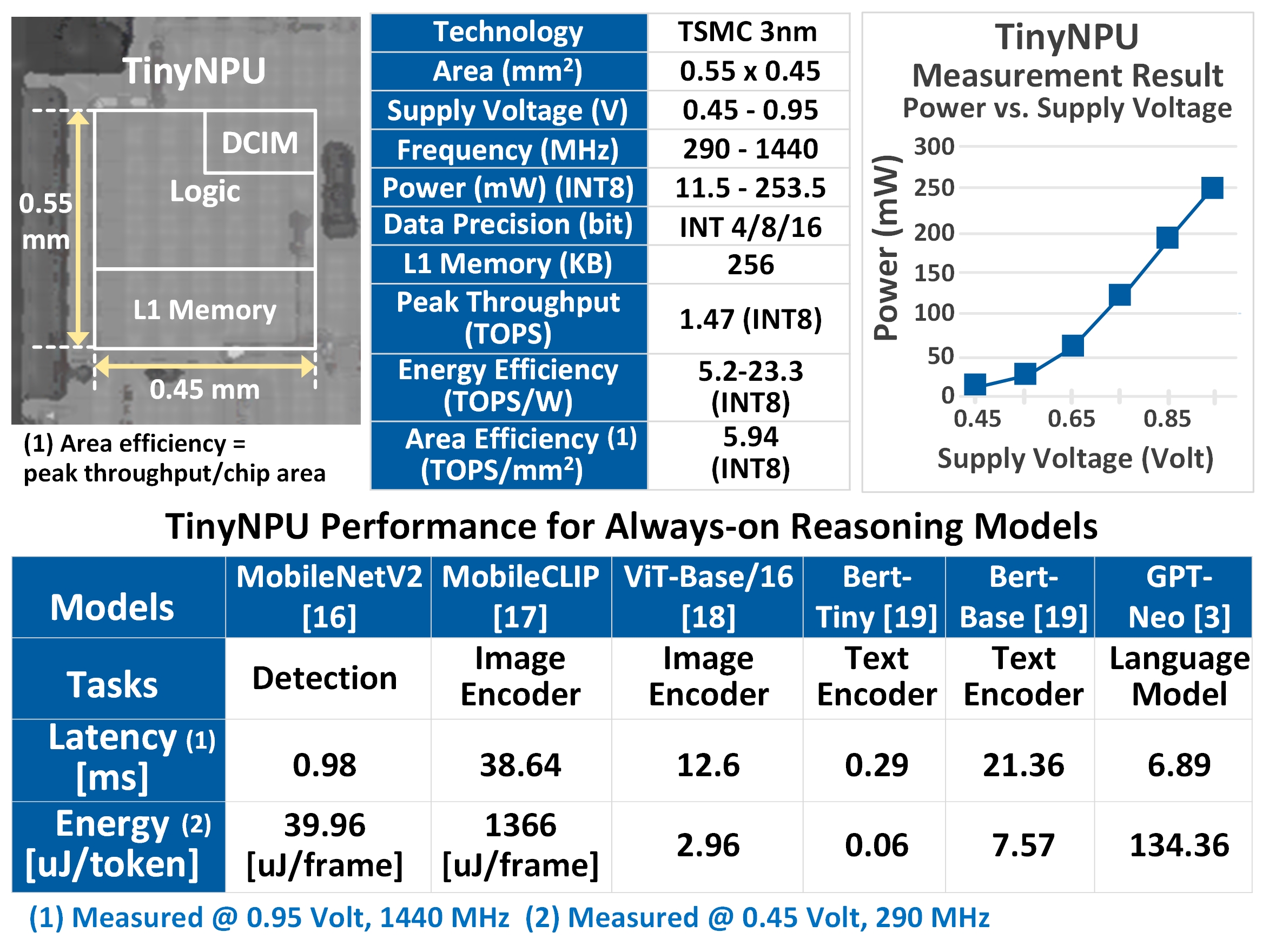
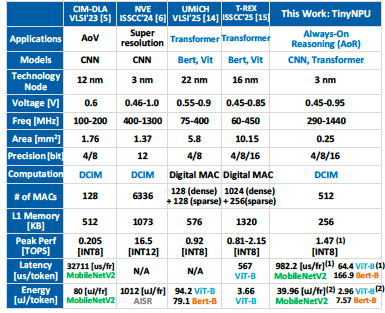
Paper C21.1, “TinyNPU: A 3nm 0.06-134.36 μJ/token DCIM-Based Ultra Low Power NPU for Always-On Reasoning on Wearables,” Y. Hsieh, E. Chang, C. Teng et al, MediaTek
Download documents and images
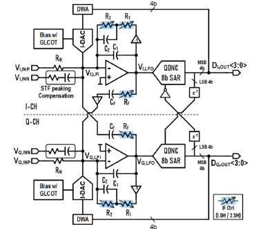
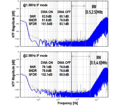
Paper C28.5, “Robust Configurable 1.5MHz / 2.5MHz IF Quadrature CT ΔΣ Modulator Using SAQB and QDNC for 175.4dB FoMs in 14nm FinFET,” Seong-Eun Cho et al, Samsung ElectronicsM Research
Download documents and images
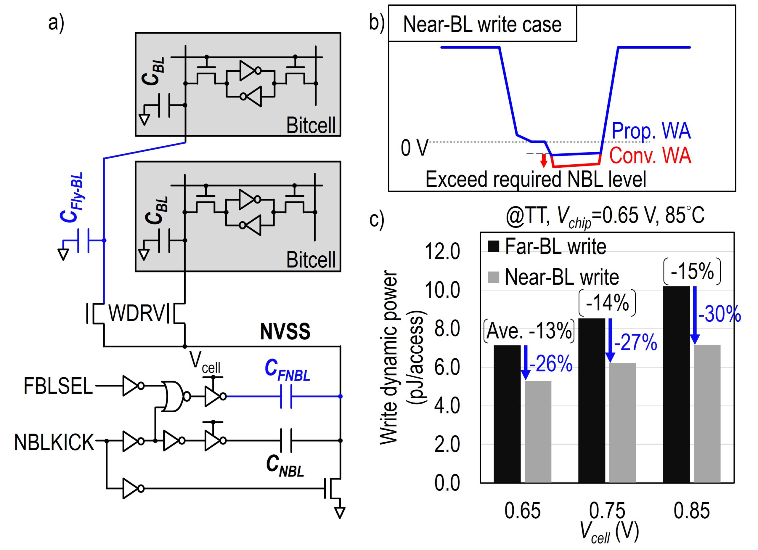
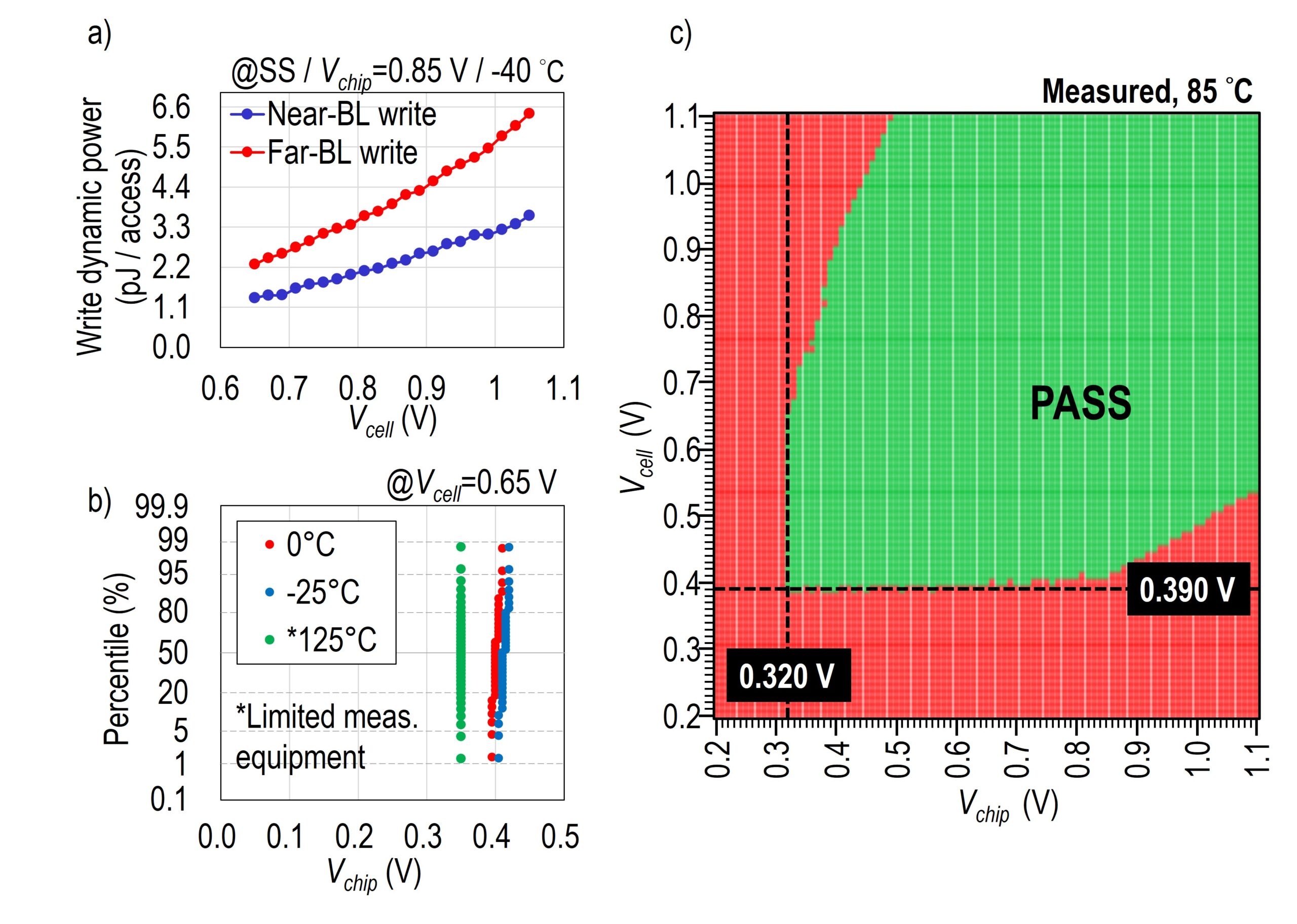
Paper C29.1, “A 2nm 37.4 Mbit/mm² Dual-Rail SRAM with Row-Access Aware Read Tracking and Write Assist Circuits Enabling 2.28pJ/Access Energy Efficient Operation,” R. Takamatsu et al, TSMC
Download documents and images